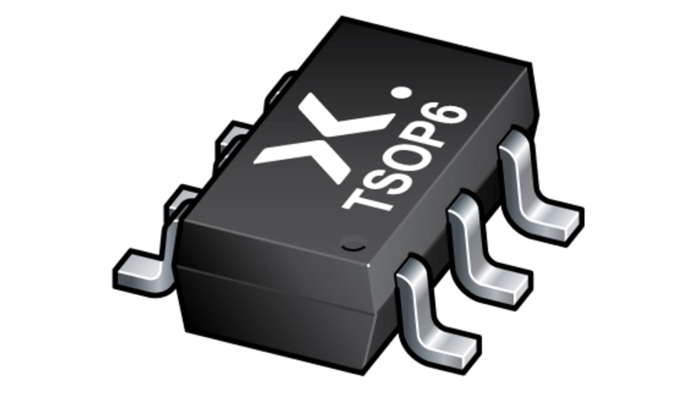
Nexperia 74LVC2G14GV,125 2 Schmitt Trigger Input CMOS Inverter, 6-Pin TSOP

This image is representative of the product range

Bulk discount available
View bulk pricing options

Subtotal (1 pack of 50 units)*

MYR22.75

Add to Basket
Select or type quantity
In Stock
  • 800 unit(s) ready to ship from another location
  • Plus 2,750 unit(s) shipping from 18 August 2026
Need more? Click ‘Check delivery dates’ to find extra stock and lead times.

Units
Per Unit
Per Pack*
50 - 700MYR0.455MYR22.75
750 - 1450MYR0.432MYR21.60
1500 +MYR0.411MYR20.55

*price indicative

Packaging Options:
RS Stock No.:
170-5382
Mfr. Part No.:
74LVC2G14GV,125
Manufacturer:
Nexperia
Find similar products by selecting one or more attributes.
Select all

Brand

Nexperia

Product Type

CMOS Inverter

Logic Function

Inverter

Input Type

Schmitt Trigger

Output Type

Schmitt Trigger

Number of Elements per Chip

2

Schmitt Trigger Input

Yes

Maximum Propagation Delay Time @ CL

7.7ns

Maximum High Level Output Current

-32mA

Maximum Low Level Output Current

32mA

Minimum Supply Voltage

1.65V

Mount Type

Surface

Maximum Supply Voltage

5.5V

Package Type

TSOP

Pin Count

6

Minimum Operating Temperature

-40°C

Logic Family

74LVC

Maximum Operating Temperature

125°C

Length

3.1mm

Height

1mm

Series

74LVC2G14

Standards/Approvals

No

Automotive Standard

No

COO (Country of Origin):
MY
The 74LVC2G14 provides two inverting buffers with Schmitt-trigger input. It is capable of transforming slowly changing input signals into sharply defined, jitter-free output signals. The inputs can be driven from either 3.3 V or 5 V devices. This feature allows the use of this device in a mixed 3.3 V and 5 V environment. Schmitt-trigger action at the inputs makes the circuit tolerant of slower input rise and fall time. This device is fully specified for partial power-down applications using IOFF.

Prevents multiple switching when driven by slow edges

Cleans up the noisy signals

Reshapes the signals in complex layouts

Suitable for mixed 3.3 V and 5.0 V applications

Wide voltage supply range

Input hysteresis

Open drain output options

CMOS and TTL variants

Overvoltage tolerant input options

Sine wave to square wave conversion

Interface between analog and digital environments

Increase noise immunity in design

Relaxation oscillators

Related links

Be the first to know about our latest products and offers

Email address

The personal information you provide to us when signing up to this mailing list will be processed in line with the Privacy Policy