Winbond SDRAM 256 MB Surface, 66-Pin 16 bit TSOP
- RS Stock No.:
- 188-2832P
- Mfr. Part No.:
- W9425G6KH-5I
- Manufacturer:
- Winbond

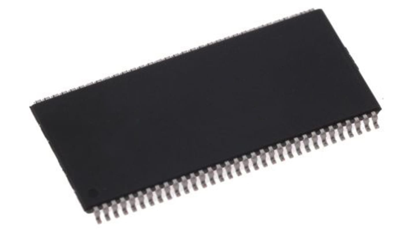
This image is representative of the product range
Currently unavailable
We don't know if this item will be back in stock, RS intend to remove it from our range soon.
- RS Stock No.:
- 188-2832P
- Mfr. Part No.:
- W9425G6KH-5I
- Manufacturer:
- Winbond
Specifications
Technical data sheets
Legislation and Compliance
Product Details
Find similar products by selecting one or more attributes.
Select all | Attribute | Value |
|---|---|---|
| Brand | Winbond | |
| Memory Size | 256MB | |
| Product Type | SDRAM | |
| Organisation | 32M x 8 Bit | |
| Data Bus Width | 16bit | |
| Address Bus Width | 15bit | |
| Number of Bits per Word | 8 | |
| Maximum Random Access Time | 55ns | |
| Number of Words | 32M | |
| Mount Type | Surface | |
| Package Type | TSOP | |
| Pin Count | 66 | |
| Minimum Operating Temperature | -40°C | |
| Maximum Operating Temperature | 85°C | |
| Length | 22.35mm | |
| Height | 1.05mm | |
| Width | 10.29 mm | |
| Series | W9425G6KH | |
| Standards/Approvals | RoHS | |
| Maximum Supply Voltage | 2.7V | |
| Minimum Supply Voltage | 2.3V | |
| Automotive Standard | No | |
| Select all | ||
|---|---|---|
Brand Winbond | ||
Memory Size 256MB | ||
Product Type SDRAM | ||
Organisation 32M x 8 Bit | ||
Data Bus Width 16bit | ||
Address Bus Width 15bit | ||
Number of Bits per Word 8 | ||
Maximum Random Access Time 55ns | ||
Number of Words 32M | ||
Mount Type Surface | ||
Package Type TSOP | ||
Pin Count 66 | ||
Minimum Operating Temperature -40°C | ||
Maximum Operating Temperature 85°C | ||
Length 22.35mm | ||
Height 1.05mm | ||
Width 10.29 mm | ||
Series W9425G6KH | ||
Standards/Approvals RoHS | ||
Maximum Supply Voltage 2.7V | ||
Minimum Supply Voltage 2.3V | ||
Automotive Standard No | ||
- COO (Country of Origin):
- TW
The W9425G6KH is a 256M DDR SDRAM and speed involving -4/-5/-5I/-5A.
Up to 250 MHz Clock Frequency
Double Data Rate architecture, two data transfers per clock cycle
Differential clock inputs (CLK and /CLK)
DQS is edge-aligned with data for Read, center-aligned with data for Write
CAS Latency: 2, 2.5, and 3
Burst Length: 2, 4 and 8
Auto Refresh and Self Refresh
Precharged Power Down and Active Power Down
Write Data Mask
Write Latency = 1
7.8μS refresh interval (8K/64 mS refresh)
Maximum burst refresh cycle: 8
Interface: SSTL_2