Winbond W972GG6KB25I SDRAM 2 GB Surface, Surface Mount, 84-Pin 16 bit WBGA
- RS Stock No.:
- 188-2584
- Mfr. Part No.:
- W972GG6KB25I
- Manufacturer:
- Winbond

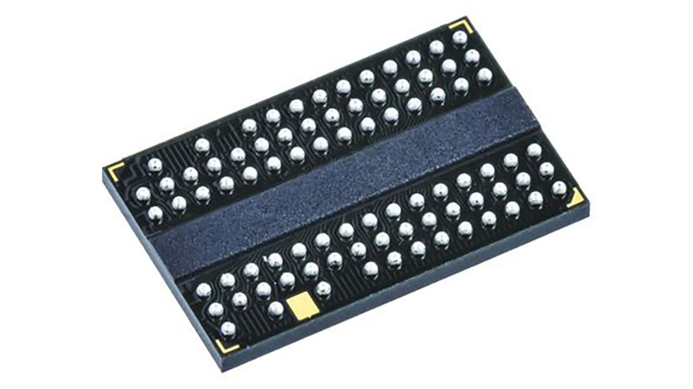
This image is representative of the product range
Currently unavailable
We don't know if this item will be back in stock, RS intend to remove it from our range soon.
- RS Stock No.:
- 188-2584
- Mfr. Part No.:
- W972GG6KB25I
- Manufacturer:
- Winbond
Specifications
Technical data sheets
Legislation and Compliance
Product Details
Find similar products by selecting one or more attributes.
Select all | Attribute | Value |
|---|---|---|
| Brand | Winbond | |
| Memory Size | 2GB | |
| Product Type | SDRAM | |
| Organisation | 256M x 8 Bit | |
| Data Bus Width | 16bit | |
| Address Bus Width | 17bit | |
| Number of Bits per Word | 8 | |
| Maximum Clock Frequency | 533MHz | |
| Maximum Random Access Time | 0.4ns | |
| Number of Words | 256M | |
| Mount Type | Surface, Surface Mount | |
| Package Type | WBGA | |
| Pin Count | 84 | |
| Minimum Operating Temperature | -40°C | |
| Maximum Operating Temperature | 95°C | |
| Standards/Approvals | RoHS | |
| Height | 0.6mm | |
| Length | 12.6mm | |
| Series | W972GG6KB | |
| Width | 8.1 mm | |
| Minimum Supply Voltage | 1.7V | |
| Supply Current | 280mA | |
| Maximum Supply Voltage | 1.9V | |
| Automotive Standard | No | |
| Select all | ||
|---|---|---|
Brand Winbond | ||
Memory Size 2GB | ||
Product Type SDRAM | ||
Organisation 256M x 8 Bit | ||
Data Bus Width 16bit | ||
Address Bus Width 17bit | ||
Number of Bits per Word 8 | ||
Maximum Clock Frequency 533MHz | ||
Maximum Random Access Time 0.4ns | ||
Number of Words 256M | ||
Mount Type Surface, Surface Mount | ||
Package Type WBGA | ||
Pin Count 84 | ||
Minimum Operating Temperature -40°C | ||
Maximum Operating Temperature 95°C | ||
Standards/Approvals RoHS | ||
Height 0.6mm | ||
Length 12.6mm | ||
Series W972GG6KB | ||
Width 8.1 mm | ||
Minimum Supply Voltage 1.7V | ||
Supply Current 280mA | ||
Maximum Supply Voltage 1.9V | ||
Automotive Standard No | ||
The W972GG6KB is a 2G bits DDR2 SDRAM, and speed involving -18, -25/25I, and -3/-3I.
Double Data Rate architecture: two data transfers per clock cycle
CAS Latency: 3, 4, 5, 6 and 7
Burst Length: 4 and 8
Bi-directional, differential data strobes (DQS and /DQS ) are transmitted / received with data
Edge-aligned with Read data and center-aligned with Write data
DLL aligns DQ and DQS transitions with clock
Differential clock inputs (CLK and /CLK)
Data masks (DM) for write data
Commands entered on each positive CLK edge, data and data mask are referenced to both edges of /DQS
Posted /CAS programmable additive latency supported to make command and data bus efficiency
Read Latency = Additive Latency plus CAS Latency (RL = AL + CL)
Off-Chip-Driver impedance adjustment (OCD) and On-Die-Termination (ODT) for better signal quality
Auto-precharge operation for read and write bursts
Auto Refresh and Self Refresh modes
Precharged Power Down and Active Power Down
Write Data Mask
Write Latency = Read Latency - 1 (WL = RL - 1)
Interface: SSTL_18