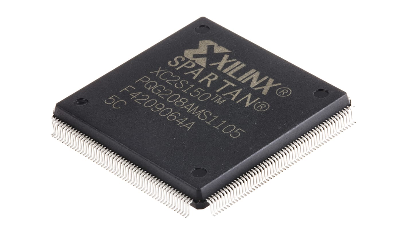
Xilinx FPGA XC2S150-5PQG208C, Spartan-II 3888 Cells, 150000 Gates, 55296bit, 864 Blocks, 208-Pin PQFP
- RS Stock No.:
- 626-0450P
- Mfr. Part No.:
- XC2S150-5PQG208C
- Manufacturer:
- Xilinx

Bulk discount available
View bulk pricing optionsSubtotal 10 units (supplied in a tray)*
MYR1,948.10
Stock information currently inaccessible - Please check back later
Units | Per Unit |
|---|---|
| 10 - 49 | MYR194.81 |
| 50 - 99 | MYR180.89 |
| 100 - 249 | MYR168.84 |
| 250 + | MYR158.29 |
*price indicative
- RS Stock No.:
- 626-0450P
- Mfr. Part No.:
- XC2S150-5PQG208C
- Manufacturer:
- Xilinx
Specifications
Technical data sheets
Legislation and Compliance
Find similar products by selecting one or more attributes.
Select all | Attribute | Value |
|---|---|---|
| Brand | Xilinx | |
| Family Name | Spartan-II | |
| Number of Logic Gates | 150000 | |
| Number of Logic Cells | 3888 | |
| Number of Logic Units | 864 | |
| Mounting Type | Surface Mount | |
| Package Type | PQFP | |
| Pin Count | 208 | |
| Number of RAM Bits | 55296bit | |
| Dimensions | 28 x 28 x 3.4mm | |
| Height | 3.4mm | |
| Length | 28mm | |
| Width | 28mm | |
| Minimum Operating Supply Voltage | 2.375 V | |
| Maximum Operating Supply Voltage | 2.625 V | |
| Minimum Operating Temperature | 0 °C | |
| Maximum Operating Temperature | +85 °C | |
| Select all | ||
|---|---|---|
Brand Xilinx | ||
Family Name Spartan-II | ||
Number of Logic Gates 150000 | ||
Number of Logic Cells 3888 | ||
Number of Logic Units 864 | ||
Mounting Type Surface Mount | ||
Package Type PQFP | ||
Pin Count 208 | ||
Number of RAM Bits 55296bit | ||
Dimensions 28 x 28 x 3.4mm | ||
Height 3.4mm | ||
Length 28mm | ||
Width 28mm | ||
Minimum Operating Supply Voltage 2.375 V | ||
Maximum Operating Supply Voltage 2.625 V | ||
Minimum Operating Temperature 0 °C | ||
Maximum Operating Temperature +85 °C | ||
- COO (Country of Origin):
- US