Altera FPGA EP2C5T144I8N Cyclone II 4608 Cells, 4608 Blocks, 144-Pin TQFP
- RS Stock No.:
- 169-5517
- Mfr. Part No.:
- EP2C5T144I8N
- Manufacturer:
- Altera

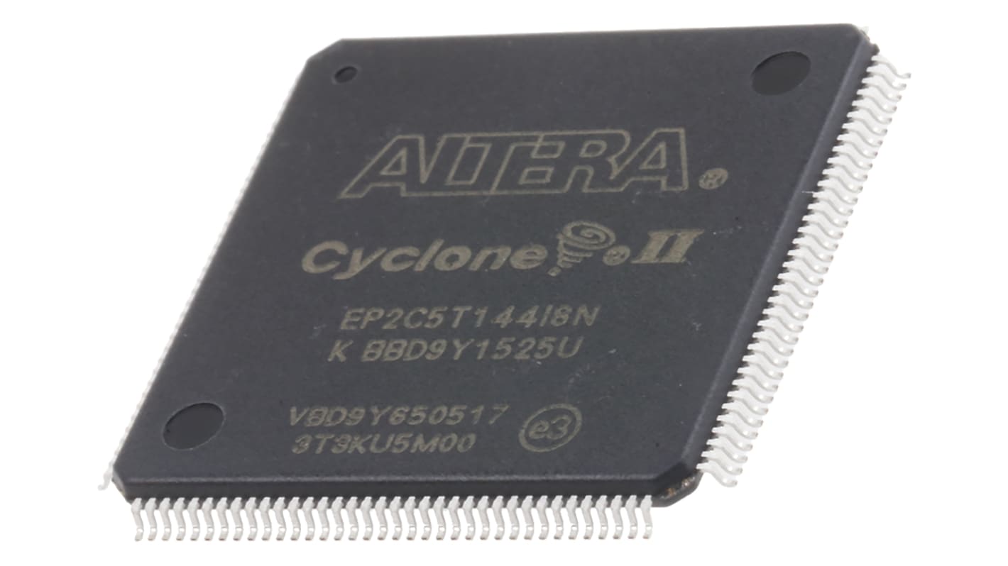
This image is representative of the product range
Subtotal (1 tray of 60 units)*
MYR14,087.64
FREE delivery for orders over RM 500.00
Temporarily out of stock
- Shipping from 24 November 2026
Need more? Click ‘Check delivery dates’ to find extra stock and lead times.
Units | Per Unit | Per Tray* |
|---|---|---|
| 60 + | MYR234.794 | MYR14,087.64 |
*price indicative
- RS Stock No.:
- 169-5517
- Mfr. Part No.:
- EP2C5T144I8N
- Manufacturer:
- Altera
Specifications
Technical data sheets
Legislation and Compliance
Product Details
Find similar products by selecting one or more attributes.
Select all | Attribute | Value |
|---|---|---|
| Brand | Altera | |
| Series | Cyclone II | |
| Product Type | FPGA | |
| Number of Logic Cells | 4608 | |
| Number of Logic Units | 4608 | |
| Number of Multipliers | 13 | |
| Mount Type | Surface | |
| Minimum Supply Voltage | 1.15V | |
| Package Type | TQFP | |
| Maximum Supply Voltage | 1.25V | |
| Pin Count | 144 | |
| Minimum Operating Temperature | -40°C | |
| Maximum Operating Temperature | 100°C | |
| Height | 1.4mm | |
| Length | 20mm | |
| Standards/Approvals | No | |
| Automotive Standard | No | |
| Select all | ||
|---|---|---|
Brand Altera | ||
Series Cyclone II | ||
Product Type FPGA | ||
Number of Logic Cells 4608 | ||
Number of Logic Units 4608 | ||
Number of Multipliers 13 | ||
Mount Type Surface | ||
Minimum Supply Voltage 1.15V | ||
Package Type TQFP | ||
Maximum Supply Voltage 1.25V | ||
Pin Count 144 | ||
Minimum Operating Temperature -40°C | ||
Maximum Operating Temperature 100°C | ||
Height 1.4mm | ||
Length 20mm | ||
Standards/Approvals No | ||
Automotive Standard No | ||
- COO (Country of Origin):
- MY
Cyclone FPGA, Altera
An FPGA is a semiconductor device consisting of a matrix of Configurable Logic Blocks (CLBs) connected through programmable interconnects. The user determines these interconnections by programming SRAM. A CLB can be simple (AND, OR gates, etc) or complex (a block of RAM). The FPGA allows changes to be made to a design even after the device is soldered into a PCB.
Related links
- Altera FPGA Cyclone II 4608 Cells 144-Pin TQFP
- Altera FPGA EP2C5T144C8N Cyclone II 4608 Cells 144-Pin TQFP
- Altera FPGA Cyclone IV E 6272 Cells 276480 bit 392 Blocks, 144-Pin EQFP
- Altera FPGA EP4CE6E22I7N Cyclone IV E 6272 Cells 276480 bit 392 Blocks, 144-Pin EQFP
- Lattice FPGA iCE40 3520 Cells 144-Pin TQFP
- Altera FPGA Cyclone III 15408 Cells 484-Pin FBGA
- Altera FPGA Cyclone IV 28848 Cells 484-Pin FBGA
- Altera FPGA Cyclone IV GX 14400 Cells 169-Pin FBGA