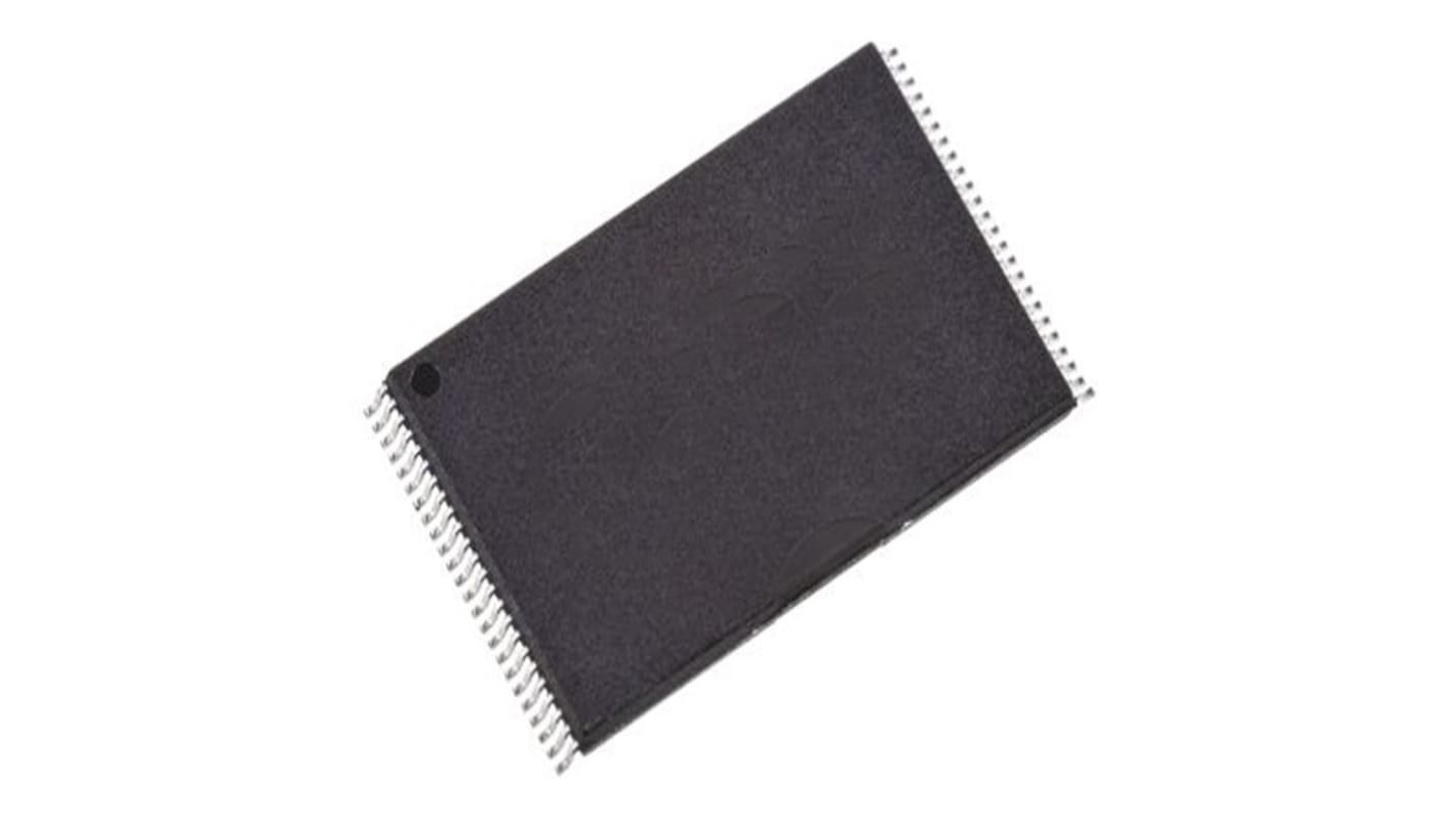
Infineon NOR 8 MB SPI Flash Memory 48-Pin TSOP
- RS Stock No.:
- 273-7519
- Mfr. Part No.:
- S29AL008J70TFI020
- Manufacturer:
- Infineon

This image is representative of the product range
Bulk discount available
Subtotal (1 pack of 2 units)*
MYR22.59
FREE delivery for orders over RM 500.00
Temporarily out of stock
- 648 left, ready to ship from another location
Need more? Click ‘Check delivery dates’ to find extra stock and lead times.
Units | Per Unit | Per Pack* |
|---|---|---|
| 2 - 8 | MYR11.295 | MYR22.59 |
| 10 - 18 | MYR10.955 | MYR21.91 |
| 20 - 48 | MYR10.52 | MYR21.04 |
| 50 - 98 | MYR9.995 | MYR19.99 |
| 100 + | MYR9.40 | MYR18.80 |
*price indicative
- RS Stock No.:
- 273-7519
- Mfr. Part No.:
- S29AL008J70TFI020
- Manufacturer:
- Infineon
Specifications
Technical data sheets
Legislation and Compliance
Product Details
Find similar products by selecting one or more attributes.
Select all | Attribute | Value |
|---|---|---|
| Brand | Infineon | |
| Memory Size | 8MB | |
| Product Type | Flash Memory | |
| Interface Type | SPI | |
| Package Type | TSOP | |
| Pin Count | 48 | |
| Maximum Clock Frequency | 133MHz | |
| Cell Type | NOR | |
| Minimum Supply Voltage | 2.7V | |
| Maximum Supply Voltage | 3.6V | |
| Minimum Operating Temperature | -40°C | |
| Maximum Operating Temperature | 125°C | |
| Standards/Approvals | No | |
| Automotive Standard | AEC-Q100 Grade 1, AEC-Q100 Grade 3 | |
| Supply Current | 20mA | |
| Series | S29AL008J | |
| Select all | ||
|---|---|---|
Brand Infineon | ||
Memory Size 8MB | ||
Product Type Flash Memory | ||
Interface Type SPI | ||
Package Type TSOP | ||
Pin Count 48 | ||
Maximum Clock Frequency 133MHz | ||
Cell Type NOR | ||
Minimum Supply Voltage 2.7V | ||
Maximum Supply Voltage 3.6V | ||
Minimum Operating Temperature -40°C | ||
Maximum Operating Temperature 125°C | ||
Standards/Approvals No | ||
Automotive Standard AEC-Q100 Grade 1, AEC-Q100 Grade 3 | ||
Supply Current 20mA | ||
Series S29AL008J | ||
The Infineon Flash Memory requires only a single 3.0 volt power supply for both read and write functions. Internally generated and regulated voltages are provided for the program and erase operations. It offers access times of up to 55 ns allowing high speed microprocessors to operate without wait states. To eliminate bus contention the device has separate chip enable, write enable and output enable controls. This Flash memory offers two power saving features. When addresses have been stable for a specified amount of time, the device enters the automatic sleep mode. The system can also place the device into the standby mode. Power consumption is greatly reduced in both these modes.
Hardware reset pin
Secured silicon sector region
Single power supply operation
Minimum 20 year data retention
Unlock bypass program command
Superior inadvertent write protection
Related links
- Infineon NOR 8 MB SPI Flash Memory 48-Pin TSOP, S29AL008J70TFI020
- Infineon NOR 8 MB SPI Flash Memory 48-Pin TSOP
- Infineon NOR 8 MB SPI Flash Memory 48-Pin TSOP, S29AL008J55TFIR20
- Infineon NOR 8 MB SPI Flash Memory Device 48-Pin TSOP
- Infineon NOR 8 MB CFI Flash Memory 48-Pin TSOP
- Infineon NOR 8 MB SPI Flash Memory Device 48-Pin TSOP, S29AL008J70BFI020
- Infineon NOR 8 MB Parallel Flash Memory 48-Pin TSOP
- Infineon NOR 8 MB CFI Flash Memory 48-Pin TSOP, S29AL008J70TFI013
