Semiconductor Packages
There are many types of semiconductor packages, varying according to their intended use. There are JEDEC and JEITA standards for semiconductor packages, but there are many packages from different semiconductor manufacturers that are not classified by these standards. Further, these JEDEC and JEITA standard names are not always used in the manufacturer’s catalogues and data sheets, and on top of that, the description system is not unified among manufacturers either.
This page provides fundamental information on the following rules regarding semiconductor package descriptions.
- Those clearly showing the same package must have unified general descriptions to the best degree possible. DIL→DIP, etc.
- In the event that there is no general designation between manufacturers, or in the event that the package is well known, the manufacturer’s description is used. PENTAWATT, etc.
- As a general rule, a number indicating the number of pins must be displayed after the package description. DIP24, SOT23-5, etc.
Note
: The information on this page is for reference. Please confirm all data on the manufacturer’s data sheet before using.
DIP
| Main classification |
Explanation of main classification |
Minor classifications |
Explanation of minor classifications |

|
Sometimes also called “DIL”, but on this site they are included in “DIP”. A type of through-hole mount package with lead pins protruding from both sides of the package. Although the pin pitch is usually 2.54mm (100mils), there are also 1.778mm (70mils) packages. Has between 6 and 64 pins. The width of the package is usually 15.2mm (600mils), 10.16mm (400mils), or 7.62mm (300mils), but please note that there are different lengths of packages even with the same number of pins. |
DIP (dual inline package) |
A plastic package DIP. Sometimes also called “PDIP”, but on this site they are included in “DIP”. |
|
CDIP (ceramic DIP) |
A ceramic package DIP. Sometimes also called “CERDIP”, but on this site they are included in “CDIP”. |
|
WDIP (DIP with window) |
A DIP with a transparent window Usually a ceramic package encased in glass. The descriptions are varied according to manufacturer, but ST Microelectronics calls them “FDIP”. On this site they are included in “WDIP”. |
|
Power DIP
|
A DIP created in such a way that it dissipates heat generated by the IC through the lead pins. Many of them use the lead pins around the center collectively as ground (earth) terminals. |
SIP
| Main classification |
Explanation of main classification |
Minor classifications |
Explanation of minor classifications |

|
Sometimes also called “SIL”, but on this site they are included in “SIP”. A type of through-hole mount package with lead pins protruding from one side of the package. When mounting onto a printed circuit board, it stands upright on the board. |
SIP (Single Inline Package) |
Has between 2 and 23 pins. There are many different shapes and pin pitches. Please note that many have special shapes with heat-dissipating structures. Its distinction from the TO220 is also not clear. |
|
ZIP (Zigzag Inline Package) |
The lead pins protruding from the side of the package are bent in a staggered fashion partway down. The pin pitch on the side of the package is 1.27mm (50mils), but becomes 2.54mm (100mils) when inserted into the printed circuit board. Has between 12 and 40 pins. |
QFP
| Main classification |
Explanation of main classification |
Minor classifications |
Explanation of minor classifications |

|
A type of surface mount package. Lead pins protrude from all four sides of the package. Characterized by the leads being in a gull wing configuration (“L” shape). There are a variety of pin pitches: 1.0mm, 0.8mm, 0.65mm, 0.5mm, 0.4mm and 0.3mm. The names are also sometimes confused. The drawback of QFP packages is that lead pins bend more easily as the pin pitch decreases. |
QFP (Quad Flat Package) |
This description is often used for standard QFP packages. |
|
FQFP (Fine pitch QFP) |
Indicates a pin pitch of less than 0.65mm. A name used by some manufacturers. |
|
HQFP (QFP with heat sink) |
QFP with heat sink (heat radiator). |
|
LQFP (Low profile QFP) |
A thin QFP with a package thickness of 1.4mm. |
|
MQFP (Metric QFP) |
A QFP classification according to the JEDEC standards. Indicates a standard QFP with a pin pitch between 1.0mm and 0.65mm and a body thickness of between 3.8mm and 2.0mm. |
|
TQFP (Thin QFP) |
A thin QFP with a height of 1.27mm (50mils) or less when mounted onto a printed circuit board. The package body has a thickness of approximately 1.00mm. A broad range of pin pitches: 0.8mm, 0.65mm, 0.5mm, and 0.4mm. Has between 44 and 120 pins. |
|
VQFP (Very small QFP) |
The name of a small QFP. The pin pitch is 0.5mm. The package body has a thickness of approximately 1.5mm. Currently incorporated in the LQFP classification, but some manufacturers still use this name. |
J-lead
| Main classification |
Explanation of main classification |
Minor classifications |
Explanation of minor classifications |

|
A type of surface mount package. Characterized by the leads being in a “J” shape. The J-shaped leads are hard to deform, and are easier to handle than QFP, etc. |
SOJ (Small Outline J-lead package) |
Lead pins protrude from two sides of the package. Has this name because the leads are shaped like the letter “J”. Usually made of plastic. Often used in memory LSI, such as DRAM, SRAM, etc. The pin pitch is 1.27mm (50mils). Has between 20 and 40 pins. |
|
PLCC (Plastic Leaded Chip Carrier) |
A plastic package with J-shaped lead pins protruding from all four sides of the package. The pin pitch is 1.27mm (50mils), and has between 18 and 84 pins. Also named in QFJ and JEITA standards. |
|
CLCC (Ceramic Leaded Chip Carrier) |
A ceramic package with J-shaped lead pins protruding from all four sides of the package. Packages with a window are used in EPROM microcomputers used to eliminate UV rays, EPROM microcomputers used in the internal organs, etc. |
|
TSOC
|
An SOJ with few pins. The pin pitch is 1.27 (50mils) like the SOJ, but it has a smaller body size. |
Grid array
| Main classification |
Explanation of main classification |
Minor classifications |
Explanation of minor classifications |

|
A package with leads arranged in a grid pattern on one side of the package. There are two types: a through-hole mount PGA type, and a surface mount BGA type. |
PGA (Pin Grid Array) |
A type of through-hole mount package. It is a package with arrayed lead pins mounted vertically on the bottom of the package, like a nailbrush. A ceramic PGA is often used when the name of the material is not particularly specified. Used in high-speed and large-scale logic LSIs. The pin pitch is 2.54mm (100mils). Has between 64 and 447 pins. There are also plastic PGAs that can be used as the base material of the package instead of glass epoxy resin printed circuit boards, in order to reduce costs. |
|
BGA (Ball Grid Array) |
A type of surface mount package. Globular solder is used on the rear side of the printed circuit board instead of arrayed leads. An LSI chip is mounted on the surface of the printed circuit board and sealed with mould resin or potting. It is an LSI package with more than 200 pins. The size of the package body can be smaller than that of QFP, and there is no concern about the leads becoming deformed. Because the lead inductance is smaller than that of QFP, it can be used in high-speed LSI packages. It is currently used in logic LSIs (between 225 and 350 pins), high-speed SRAM (119-pin, etc.), and so forth. |
|
Micro SMD
|
A small BGA package developed by National Semiconductor. Has between 4 and 42 pins. |
SO
| Main classification |
Explanation of main classification |
Minor classifications |
Explanation of minor classifications |

|
“SO” stands for “Small Outline”. It is a surface mount package with gull wing (L-shaped) leads protruding from two sides of the package. There are a variety of descriptions for these types of packages. Please note that even packages with the same name may have different shapes. |
SOP (Small Outline Package) |
Those with a pin pitch of 1.27mm (50mils) are called “SOP” in the JEITA standards. Please note that those called “SOP” in the JEDEC standards have different widths. |
|
SOIC (Small Outline Integrated Circuit) |
Sometimes also called “SO” or “SOL”, but on this site they are included in “SOIC”. Those with a pin pitch of 1.27mm (50mils) are called “SOIC” in the JEDEC standards. Please note that those called “SOIC” in the JEITA standards have different widths. |
|
MSOP (Mini (Micro) SOP) |
A small SOP with a pin pitch of 0.65mm or 0.5mm. Analog Devices calls them “microSOIC”, Maxim calls them “SO/uMAX”, and national Semiconductor calls them “MiniSO”. |
| Can also be considered SSOP or TSSOP. |
|
QSOP (Quarter SOP) |
A small SOP with a pin pitch of 0.635mm (25mils). |
|
SSOP (Shrink SOP) |
A narrow, small SOP with a pin pitch of 1.27mm (50mils). There are SSOPs with pin pitches of 1.0mm, 0.8mm, 0.65mm, and 0.5mm. Has between 5 and 80 pins. They are widely used as small surface mount packages. |
|
TSOP (Thin SOP) |
A thin small outline package. An SOP with a height of 1.27mm (50mils) or less when mounted and a pin pitch of 1.27mm or less. Has between 24 and 64 pins. There are two types of TSOP: one in which the lead terminals are mounted on the short sides of the package (pin pitch of 0.6mm, 0.55mm, or 0.5mm), and one in which the lead terminals are mounted on the long sides of the package (regular pin pitch of 1.27mm). The former is called “type I” and the latter “type II” in the JEITA standards. |
|
TSSOP (Thin Shrink SOP) |
A thin SSOP with a package thickness of 1.0mm. The pin pitch is 0.65mm or 0.5mm, and has between 8 and 56 pins. |
|
HTSSOP (TSSOP with Heat slug) |
A heat dissipation surface called a “thermal pad” is provided on the surface of the TSSOP board mounting side. |
|
CERPAC
|
A ceramic sealed package. The pin pitch is 1.27mm (50mils). |
|
DMP
|
A New Japan Radio (called “NJR” on this site) package. The pin pitch is 1.27mm (50mils) and it is similar to SOP and SOIC, but the width of the package is different. |
|
SC70
|
Can also be considered a type of SSOP. A small surface mount package with a pin pitch of 0.65mm. Most have 5 pins, but there is also a 6-pin variety. Depending on the manufacturer, it is also called “USV” or “CMPAK”. |
SOT
| Main classification |
Explanation of main classification |
Minor classifications |
Explanation of minor classifications |
|
“SOT” stands for “Small Outline Transistor”. It was originally a small transistor surface mount package. Depending on the manufacturer, a different name may be used, even if it has the same shape as SOT. |
SOT23
|
A small surface mount package with a pin pitch of 0.95mm. Has between 3 and 6 pins. Depending on the manufacturer, it is also called “SC74A”, “MTP5”, “MPAK”, or “SMV”. |
|
SOT89
|
A small surface mount package with a pin pitch of 1.5mm and a heat dissipation tab. Most have 3 pins, but there is also a 5-pin variety. Depending on the manufacturer, it is also called “UPAK”. |
|
SOT143
|
A small surface mount package with a pin pitch of 1.9mm. Has 4 pins. One of the pins is wider than the others. |
|
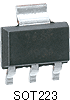
SOT223
|
A small surface mount package with a pin pitch of 2.3mm and a heat dissipation tab. Has 3 pins. |
TO (plastic)
| Main classification |
Explanation of main classification |
Minor classifications |
Explanation of minor classifications |

|
“TO” stands for “Transistor Outline”. It was originally a transistor package. It is designed such that the leads can be formed and used for surface mounting. Depending on the manufacturer, a different name may be used, even if it has the same shape as TO. |
TO3P
|
A package used in voltage regulators, etc. It was originally a transistor package. |
|
TO92
|
A package used in voltage regulators, voltage references, etc. It was originally a transistor package. There are variations, such as “mini size” and “long body”. Also called “TO226AA” in the JEDEC standards. |
|
TO220
|
A package used in voltage regulators, etc. It was originally a transistor package. Has a tab used for mounting it to a heat sink. There are also full mold types in which the tab is covered with plastic. There are also varieties with many pins, used in amps and so forth. ST Microelectronics’ PENTAWATT (5 pins), HEPTAWATT (7 pins), and MULTIWATT (many pins), etc. are classified as types of TO220, but they can also be considered a part of SIP. |
|
TO252
|
A package used in voltage regulators, etc. It was originally a transistor package. Some manufacturers also call long lead parts “SC64”. Those that have been designed such that the leads can be formed and used for surface mounting are also called “DPAK”, “PPAK”, or “SC63” by some manufacturers. |
|
TO263
|
Similar to the TO220, but with a smaller tab. Usually designed such that the leads can be formed and used for surface mounting. Besides 3-pin, there are also 5-pin and 7-pin varieties. Also called “D2PAK (DDPAK)”. |
TO (CAN)
| Main classification |
Explanation of main classification |
Minor classifications |
Explanation of minor classifications |

|
A metal case (CAN) package. There is no surface mount component. The leads are connected through the printed circuit board. Now rarely used. |
TO3
|
An early power transistor package. Fixed to a heat sink with two screws. |
|
TO5
|
A cylindrical metal package with a diameter of 8mm and height of 4mm. Similar to T039. |
|
TO39
|
A cylindrical metal package with a diameter of 8mm and height of 4mm. Similar to T05. |
|
TO46
|
A cylindrical metal package with a diameter of 5mm and height of 2.5mm. Slightly shorter than TO52. |
|
TO52
|
A cylindrical metal package with a diameter of 5mm and height of 3.5mm. Slightly taller than TO46. |
|
TO99
|
A cylindrical metal package with a diameter of 8mm and height of 4mm. Eight pins are arranged in a circle on the bottom, in the center of which is a 1mm protrusion to keep the bottom raised from the printed circuit board. Its external form is similar to that of TO100. |
|
TO100
|
A cylindrical metal package with a diameter of 8mm and height of 4mm. Ten pins are arranged in a circle on the bottom, in the center of which is a 1mm protrusion to keep the bottom raised from the printed circuit board. Its external form is similar to that of TO99. |